How to Optimize the Flex Circuit Manufacturer Process for Cost
Flex Circuit Manufacturer Process for Cost
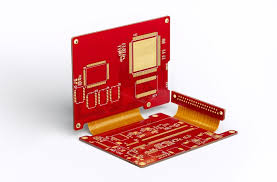
A flex circuit, also known as a flexible printed circuit (FPC), is similar to a standard PCB but includes conductive traces that bend. These traces connect the components and allow for the circuit to be mounted to other products. These conductive paths can be etched into a thin, flexible copper sheet.
When compared to traditional rigid PCBs, flex circuits are usually more complex and have higher cost, but the benefits of flex circuits can make them worth the investment for many manufacturers. To maximize the product’s value, it is important to optimize the flex circuit manufacturer process for cost in order to keep costs down and production time up.
One of the most significant factors in determining a flex circuit’s cost is the material selection. High quality materials can provide better durability and performance. Choosing cheap materials may save manufacturing costs, but they can decrease the reliability and longevity of the final product. A reputable flex circuit manufacturer will help you determine the right material for your specific application.
The base layer for a flex circuit is usually an epoxy or polyimide substrate. A flex circuit manufacturer uses different materials for the core and coverlay layers, depending on the design requirements. For example, a low volume and prototype run can use inexpensive PET or PEN films, while higher-reliability flex circuits require premium fluoropolymer films.
How to Optimize the Flex Circuit Manufacturer Process for Cost
During the fabrication process, the copper foil is annealed to increase its flexibility and strength. This annealing is done by running the copper through high-pressure rollers that elongate the grain structure in a planar direction. This enables the conductors to bend without breaking. The flex circuit can be further reinforced with stiffeners if needed.
When designing a flex circuit, it is important to keep the layer count down to avoid unnecessary manufacturing costs. Denser flex circuit layouts add complexity and may not be necessary for your application. It is also important to consider the layout of your vias. Advanced holes like blind and buried vias can increase your cost, but are often necessary for certain designs.
To minimize stress on the flex circuits during bending, designers should stagger the placement of through-holes and component placement near bend areas. Also, it is a good idea to use rounded corners for the edges of the expected/designed bending area. This reduces strain and increases the tear resistance compared to 90 degree sharp corners.
A flex circuit requires an additional layer of film to protect the outer surface of the copper, similar to a solder mask on a rigid PCB. The most common coverlay is an additional layer of polyimide, but there are also adhesive-less processes available. In addition to protecting the outer surface, this layer can act as a signal insulator. In most cases, the coverlay is applied by using a photo-imageable solder mask, but for coarser designs, screen printing may be used. In any case, the coverlay must be clearly shown in the flex circuit fabrication drawings.